Geometric design and modelling of wafer patterning, minimizing residual thermal strain and wafer bowing

Optimization of epitaxial growth processes of 3C-SiC

Growth of real bulk size 3C-SiC crystals with a thickness of several mm

Device concepts with potential for operation in high temperature and high radiation environments


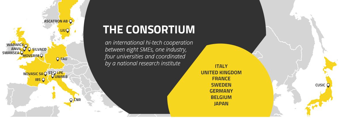

CHALLENGE project - 3C-SiC Hetero-epitaxiALLy grown on silicon compliancE substrates and 3C-SiC substrates for sustaiNable wide-band-Gap powEr devices - has received funding from the EU's H2020 framework programme for research and innovation under grant agreement n. 720827 from 1/1/2017 to 31/12/2020.
Funded under: H2020-EU.2.1.3. - INDUSTRIAL LEADERSHIP - Leadership in enabling and industrial technologies - Advanced materials